M.Sc – Application of Artificial Intelligence to Electronic Design Automation
Many Electronic Design Automation (EDA) processes are known to be either NP-Complete or NP-Hard, meaning that optimal solutions can neither be found nor verified in polynomial time. Consequently, the goal becomes to find a good enough solution, which essentially divides the techniques into two categories based on how the objective function, gauging the performance of the result, is formulated. First, if the objective function can be represented as a differentiable function, analytic techniques can be used to minimise the error gradient and quickly arrive at a solution. In the alternative approach, the objective function is non-differentiable, and metaheuristics are often employed. These black-box optimisation techniques are driven by stochastic decision-making, which has been empirically proven to yield good results. Generally speaking, the more comprehensive the objective function, the more challenging it becomes to formulate in a differentiable manner and take advantage of analytic techniques.
Limiting our scope to the placement task in Printed Circuit Board (PCB) physical design, the following observations motivated our research: Stochastic placement techniques are ubiquitous in this space, mainly because the problems are small (100s-1000s of components), but they always start searching from scratch and do not yield satisfactory layouts by the standards of hardware design engineers. We conducted basic research to identify novel learning-based methods for achieving objectively good performance while delivering practically acceptable layouts. We apply Reinforcement Learning (RL) to solve such optimisation problems in an end-to-end manner under the guidance of a non-differential reward function.
The following results exhibit how the resulting policies not only demonstrate an understanding of fundamental placement techniques but also show emergent behaviour. We refer interested readers to our related published works and accompanying open-source code.


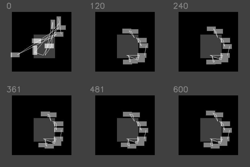
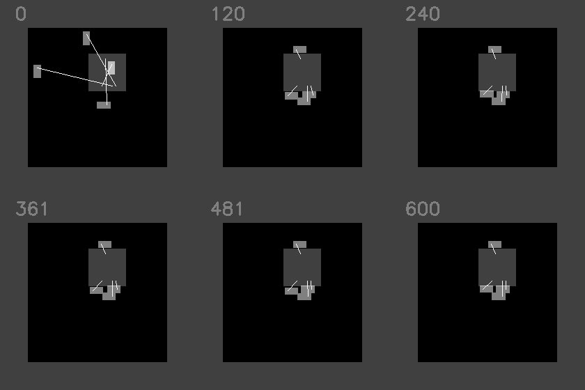

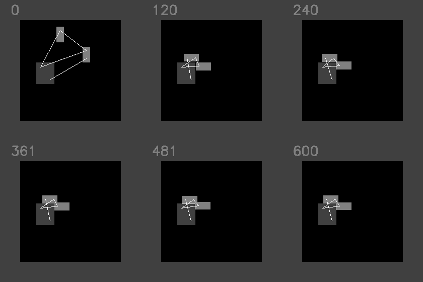
Figure: Illustration of various learned policies for optimising the placement of components on a PCB. The reward function guides the learning process and comprises the linear combination of Euclidean Wirelength (EW), Half-Perimeter Wirelength (HPWL) and Overlap. The assigned values noted in each Sub Figure represent their contribution.
Do you find this research Interesting?
If you’re intrigued by EDA and the bio-inspired concepts of emergence and complexification, here are a few exciting areas where this research can really thrive.
Placement: Elegant Circuit Placement Solutions through Reinforcement Learning and Complexification
Routing: A Learning based distributed routing algorithm for constraint-driven placement
Publications
L. Vassallo and J.Bajada, Learning Circuit Placement Techniques through Reinforcement Learning with Adaptive Rewards, Design Automation and Test in Europe (DATE’24), Valencia, Spain, March 2024. (Paper, video, code)
L. Vassallo, Automated PCB Component Placement using Reinforcement Learning, University of Malta, 2023 (Thesis)
Source Code
RL PCB – A novel learning-based method for optimising the placement of circuit components on a PCB.